

Original on-chip bus for combining hundreds of processing cores has been developed
- Details
- Published: Monday, 08 April 2013 10:17
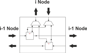 |
SPBUS hub scheme |
The development of simple packet bus (SPBUS), enabling to ensure connectivity of hundreds of different devices inside a chip, is finished. SPBUS implementation is written entirely on VHDL without using closed source licensed IP. The developed bus is exceptionally compact in terms of FPGA or VLSI hardware resources usage, along with that it provides delays less than 50 cycles during data transfer.
Although we call SPBUS a bus, it would be terminologically correct to name it “a switch tree”. Each SPBUS hub has 3 input and 3 output ports. Each device or each node on the chip is equipped with its own switch. One input port and one output port of each hub are plugged to current node, the rest of the ports provide data transfer with adjacent node hubs.
Data is transferred through the bus using wormhole method. The essence of the method is this: when the first part of a package can’t be sent further, there is a signal to the sending side to stop the transmission until the path is clear. The signal limits sending messages for certain time. Such type of control is called ‘back pressure control’. This approach enables to minimize the amount of hub buffer memory.
The bus has been developed with taking into account the GALS (Globally Asynchronous Locally Synchronous) concept. This concept implies partition the network into domains with independent clocking control. Dual-port memory blocks are applied to cross the borders of clock domains for data transfer. In order to simplify the dual-port system, computing node local memory has been created.
