

We've started to create the MALT-Cv1 netlist using 28 nanometer TSMC technology
- Details
- Published: Monday, 16 May 2016 20:38
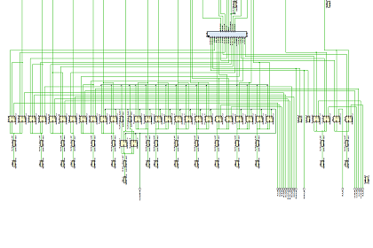 |
Fragment of digital citcuit Photo: maltsystem.com |
We've started to create the MALT-Cv1 netlist using 28 nanometer HPC+ (high-performance computing) TSMC technology. Planned area of a chip - 12 mm2. Such area is ecological optimum for pilot batch manufacturing under MPW (Multi-Project Wafer). Estimated energy consumption on a target task is 1 W, which enables to achieve considerably higher energy efficiency calculations than on a CPU and GPU. In order to achieve high performance of energy efficiency design, automated design route for VLSI has been customized via CAD Cadence Genus Synthesis Solution and Cadence Incisive Enterprise Simulator, allowing to obtain estimates of energy right after RTL editing on real switching activity of triggers.
